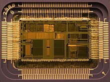
486 DX

The exposed die of an Intel 80486DX2 microprocessor
|
|
| Produced | From 1989 to 2007 |
|---|---|
| Common manufacturer(s) |
|
| Max. CPU clock rate | 16 MHz to 150 MHz |
| FSB speeds | 16 MHz to 50 MHz |
| Min. feature size | 1 µm to 0.6 µm |
| Instruction set | x86 including x87 (except for "SX" models) |
| Data width | 32 |
| Address width | 32 |
| Virtual address width | 32 Linear; 46 Logical |
| Predecessor | Intel 80386 |
| Successor | Pentium (P5) |
| Co-processor | Intel 80487SX |
| Package(s) | |
| Intel 80486 registers | ||||||||||||||||||||||||||||||||||||||||||||||||||||||||||||||||||||||||||||||||||||||||||||||||||||||||||||||||||||||||||||||||||||||||||||||||||||||||||||||||
|
||||||||||||||||||||||||||||||||||||||||||||||||||||||||||||||||||||||||||||||||||||||||||||||||||||||||||||||||||||||||||||||||||||||||||||||||||||||||||||||||
|
||||||||||||||||||||||||||||||||||||||||||||||||||||||||||||||||||||||||||||||||||||||||||||||||||||||||||||||||||||||||||||||||||||||||||||||||||||||||||||||||
|
||||||||||||||||||||||||||||||||||||||||||||||||||||||||||||||||||||||||||||||||||||||||||||||||||||||||||||||||||||||||||||||||||||||||||||||||||||||||||||||||
The Intel 80486, also known as the i486 or 486 ("four-eighty-six"), is a higher performance follow-up to the Intel 80386 microprocessor. The 80486 was introduced in 1989 and was the first tightlypipelined x86 design as well as the first x86 chip to use more than a million transistors, due to a large on-chip cache and an integrated floating-point unit. It represents a fourth generation of binary compatible CPUs since the original 8086 of 1978.
A 50 MHz 80486 executes around 40 million instructions per second on average and is able to reach 50 MIPS peak performance.
The i486 does not have the usual 80-prefix because of a court ruling that prohibits trademarking numbers (such as 80486). Later, with the introduction of the Pentium brand, Intel began branding its chips with words rather than numbers.
The 80486 was announced at Spring Comdex in April 1989. At the announcement, Intel stated that samples would be available in the third quarter of 1989 and production quantities would ship in the fourth quarter of 1989. The first 80486-based PCs were announced in late 1989, but some advised that people wait until 1990 to purchase a 80486 PC because there were early reports of bugs and software incompatibilities.
The instruction set of the i486 is very similar to its predecessor, the Intel 80386, with the addition of only a few extra instructions, such as CMPXCHG which implements a compare-and-swap atomic operation and XADD, a fetch-and-add atomic operation returning the original value (unlike a standard ADD which returns flags only).
From a performance point of view, the architecture of the i486 is a vast improvement over the 80386. It has an on-chip unified instruction and data cache, an on-chip floating-point unit (FPU) and an enhanced bus interface unit. Due to the tight pipelining, sequences of simple instructions (such as ALU reg,reg and ALU reg,im) could sustain a single clock cycle throughput (one instruction completed every clock). These improvements yielded a rough doubling in integer ALU performance over the 386 at the same clock rate. A 16-MHz 80486 therefore had a performance similar to a 33-MHz 386, and the older design had to reach 50 MHz to be comparable with a 25-MHz 80486 part.
...
Wikipedia
