Tungsten diselenide
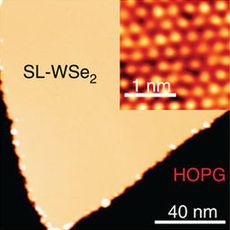
 WSe2 monolayer on graphite (yellow) and its atomic image (inset)
|
|
 |
|
| Identifiers | |
|---|---|
|
3D model (JSmol)
|
|
| ECHA InfoCard | 100.031.877 |
| EC Number | 235-078-7 |
|
PubChem CID
|
|
|
|
|
|
| Properties | |
| WSe2 | |
| Molar mass | 341.76 g/mol |
| Appearance | grey to black solid |
| Odor | odorless |
| Density | 9.32 g/cm3 |
| Melting point | > 1200 °C |
| insoluble | |
| Band gap | ~1 eV (indirect, bulk) ~1.7 eV (direct, monolayer) |
| Structure | |
|
hP6, space group P6 3/mmc, No 194 |
|
|
a = 0.3297 nm, c = 1.2982 nm
|
|
|
Trigonal prismatic (WIV) Pyramidal (Se2−) |
|
| Hazards | |
| Main hazards | External MSDS |
|
Except where otherwise noted, data are given for materials in their standard state (at 25 °C [77 °F], 100 kPa).
|
|
| Infobox references | |
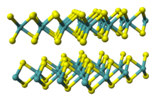
Tungsten diselenide is an inorganic compound with the formula WSe2. The compound adopts a hexagonal crystalline structure similar to molybdenum disulfide. Every tungsten atom is covalently bonded to six selenium ligands in a trigonal prismatic coordination sphere while each selenium is bonded to three tungsten atoms in a pyramidal geometry. The tungsten–selenium bond has a length of 0.2526 nm, and the distance between selenium atoms is 0.334 nm. Layers stack together via van der Waals interactions. WSe2 is a very stable semiconductor in the group-VI transition metal dichalcogenides.
Heating thin films of tungsten under pressure from gaseous selenium and high temperatures (>800 K) using the sputter deposition technique leads to the films crystallizing in hexagonal structures with the correct stoichiometric ratio.
Transition metal dichalcogenides are semiconductors with potential applications in solar cells. WSe
2 has a band-gap of ~1.35 eV with a temperature dependence of −4.6×10⁻⁴ eV/K.WSe
2 photoelectrodes are stable in both acidic and basic conditions, making them potentially useful in electrochemical solar cells.
The properties of WSe
2 monolayers differ from those of the bulk state, as is typical for semiconductors. Mechanically exfoliated monolayers of WSe
2 are transparent photovoltaic materials with LED properties. The resulting solar cells pass 95 percent of the incident light, with one tenth of the remaining five percent converted into electrical power. The material can be changed from p-type to n-type by changing the voltage of an adjacent metal electrode from positive to negative, allowing devices made from it to have tunable bandgaps. As a result, it may enable LEDs of any color to be made from a single material.
...
Wikipedia
