Intel i860
| Designer | Intel |
|---|---|
| Bits | 32/64-bit |
| Introduced | 1989 |
| Design | RISC, VLIW |
| Type | Register-Register |
| Encoding | Fixed |
| Branching | Compare and branch |
| Endianness | Bi |
| Page size | 4 KiB |
| Extensions | 64-bit graphics unit |
| Registers | |
| General purpose | 32 32-bit |
| Floating point | 32 32-bit (16 64-bit) |

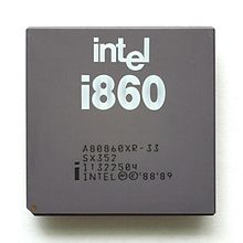
Intel i860 XR microprocessor (33 MHz edition)
|
|
| Produced | From 1989 to mid-1990s |
|---|---|
| Common manufacturer(s) |
|
| Max. CPU clock rate | 25 MHz to 40 MHz |
| Instruction set | Intel i860 |
| Cores | 1 |
| L1 cache | 4 KB (I) + 8 KB (D) |
| Successor | i860 XP |

Intel i860 microprocessor (50 MHz edition)
|
|
| Produced | From 1991 to mid-1990s |
|---|---|
| Common manufacturer(s) |
|
| Max. CPU clock rate | 40 MHz to 50 MHz |
| Instruction set | Intel i860 |
| Cores | 1 |
| L1 cache | 16+16 KB |
| Predecessor | i860 XR |
The Intel i860 (also known as 80860) was a RISC microprocessor design introduced by Intel in 1989. It was one of Intel's first attempts at an entirely new, high-end instruction set architecture since the failed Intel i432 from the 1980s. It was released with considerable fanfare, slightly obscuring the earlier Intel i960, which was successful in some niches of embedded systems, and which many considered to be a better design. The i860 never achieved commercial success and the project was terminated in the mid-1990s.
The first implementation of the i860 architecture was the i860 XR microprocessor (code named N10), which ran at 25, 33, or 40 MHz. The second-generation i860 XP microprocessor (code named N11) added 4 Mbyte pages, larger on-chip caches, second level cache support, faster buses, and hardware support for bus snooping, for cache consistency in multiprocessor systems. A process shrink for the XP (from 1 micrometre to 0.8 CHMOS V) bumped it to 40 and 50 MHz. Both microprocessors supported the same instruction set for application programs.
The i860 combined a number of features that were unique at the time, most notably its very long instruction word (VLIW) architecture and powerful support for high-speed floating point operations. The design mounted a 32-bit ALU "Core" along with a 64-bit FPU that was itself built in three parts: an adder, a multiplier, and a graphics processor. The system had separate pipelines for the ALU, floating point adder and multiplier, and could hand off up to three operations per clock. (I.e., two instructions - one integer instruction and one floating point multiply-and-accumulate instruction per clock.)
All of the buses were at least 64 bits wide. The internal memory bus to the cache, for instance, was 128 bits wide. Both units had thirty-two 32-bit registers, but the FPU used its set as sixteen 64-bit registers. Instructions for the ALU were fetched two at a time to use the full external bus. Intel referred to the design as the "i860 64-Bit Microprocessor".
...
Wikipedia
