GeForce 10 series

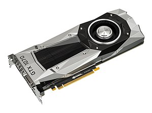
The GTX 1070 Founders Edition reference card.
|
|
| Release date | May 2016 |
|---|---|
| Codename | GP10x |
| Architecture | Pascal |
| Models | GeForce GTX Series |
| Transistors and fabrication process |
|
| Cards | |
| Entry-level | GeForce GT 1030 GeForce GTX 1050 GeForce GTX 1050 Ti |
| Mid-range | GeForce GTX 1060 |
| High-end | GeForce GTX 1070 GeForce GTX 1080 |
| Enthusiast | GeForce GTX 1080 Ti NVIDIA TITAN X NVIDIA TITAN Xp |
| API support | |
| Direct3D | Direct3D 12.0 (feature level 12_1) |
| OpenCL | OpenCL 1.2 |
| OpenGL | OpenGL 4.5 |
| Vulkan |
Vulkan 1.0 SPIR-V |
| History | |
| Predecessor | GeForce 900 series |
GeForce GTX 10 Series is a series of graphics processing units developed by Nvidia, based on Nvidia's Pascal microarchitecture, serving as a successor to the GeForce 900 Series.
The Pascal microarchitecture, named after the 17th-century French mathematician Blaise Pascal, was presented on May 6, 2016. It is the successor to the Maxwell microarchitecture and incorporates TSMC's 16 nm FinFET technology. It also incorporates Samsung's 14 nm FinFET technology for Nvidia's GP107 chips.
New Features in GP10x:
Nvidia has announced that the Pascal GP100 GPU will feature four High Bandwidth Memory stacks, allowing a total of 16 GB HBM2 on the highest-end models, 16 nm technology,Unified Memory and NVLink.
After Pascal, the next architecture will be codenamed Volta, after the 18th century Italian physicist Alessandro Volta. Volta was to be the direct successor to Maxwell but in 2014 Nvidia announced that Pascal was following Maxwell "to take advantage of stacked memory and other innovations sooner." On May 11, 2017, Nvidia announced the first Volta-powered GPU, the Tesla V100 datacenter-targeted card. The GPU in the V100, built using a 12-nanometer manufacturing process, measures 815 square mm. and features 21 billion transistors, 5120 CUDA cores running at 1455MHz boost clock, and 640 “tensor cores”, specialized in deep learning. The card features NVLink 2.0, and 16GB of 4096-bit second-gen HBM2, which features peak speeds of 900 GB/s.
...
Wikipedia
