Etching (microfabrication)
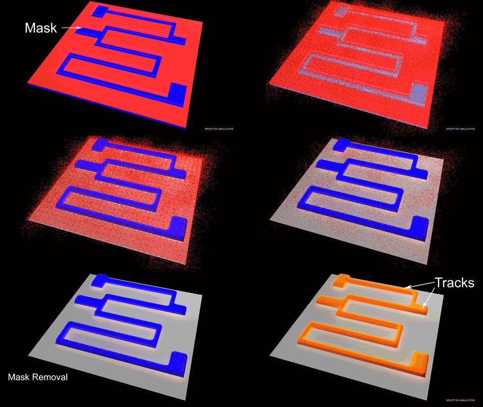
Etching is used in microfabrication to chemically remove layers from the surface of a wafer during manufacturing. Etching is a critically important process module, and every wafer undergoes many etching steps before it is complete.
For many etch steps, part of the wafer is protected from the etchant by a "masking" material which resists etching. In some cases, the masking material is a photoresist which has been patterned using photolithography. Other situations require a more durable mask, such as silicon nitride.
If the etch is intended to make a cavity in a material, the depth of the cavity may be controlled approximately using the etching time and the known etch rate. More often, though, etching must entirely remove the top layer of a multilayer structure, without damaging the underlying or masking layers. The etching system's ability to do this depends on the ratio of etch rates in the two materials (selectivity).
Some etches undercut the masking layer and form cavities with sloping sidewalls. The distance of undercutting is called bias. Etchants with large bias are called isotropic, because they erode the substrate equally in all directions. Modern processes greatly prefer anisotropic etches, because they produce sharp, well-controlled features.
The two fundamental types of etchants are liquid-phase ("wet") and plasma-phase ("dry"). Each of these exists in several varieties.
The first etching processes used liquid-phase ("wet") etchants. The wafer can be immersed in a bath of etchant, which must be agitated to achieve good process control. For instance, buffered hydrofluoric acid (BHF) is used commonly to etch silicon dioxide over a silicon substrate.
...
Wikipedia

